36 schottky diode band diagram
PDF Graphene Schottky diodes: an experimental review of the rectifying... Schottky diodes are important electronic components, used in many applications such as solar cells, photodetectors, clamped transistors, MESFETs equilibrium band diagram for the M/S junction. The physical junction is set at x = 0 . Fi is the energy. barrier to the flow of electrons (black dots) from the... PDF Schottky Diode Schottky Diode. Features: • Low power loss, high efficiency • High current capability, low VF • High reliability • High surge current : DO-41 moulded plastic : Pure tin plated, lead free, solderable per MIL-STD-202, Method 208 guaranteed : Colour band denotes cathode end : 260°C/10 seconds/0.375"...
Energy band diagram of a metal-semiconductor Schottky diode with... Schottky Diodes, Channels and Bias (Epidemiology) | ResearchGate, the professional network for scientists. Near-infrared radiation of wavelength 1.5 μm is up-converted to a visible wavelength of 818 nm by internal photoemission in a Schottky diode with a modulation p-doped channel.
Schottky diode band diagram
PDF Broadband schottky diode 2 Schottky Diode Technology for Frequency Multipliers. 145 5.9 Block diagram for the W -band fundamental mixer measurement. . . . 145 5.10 Measured output power across W -band for 100 mW input power. . . . Schottky Diodes - Working, Characteristics, Application - Homemade... Schottky diodes are constructed differently compared to the traditional p-n junction diodes. Instead of a p-n junction they are built using a metal In Schottky diodes electrons become the majority carrier in the semiconductor material, while in the metal exhibits extremely small minority carriers (holes). Schottky Diode - Function, Construction, Characteristics, Applications... A Schottky diode, widely popular as barrier diode, refers to a metal-semiconductor diode that comprises lower voltage drops than usual PN-junction diodes. The following diagram represents the Schottky diode symbol -. [Image will be Uploaded Soon]. In the above diagram, the anode section...
Schottky diode band diagram. Schottky Diode: What is it? (Symbol, Applications...) | Electrical4U A SIMPLE explanation of Schottky Diodes (hot-carrier diode or Schottky barrier diode). Learn what a Schottky Diode is, the symbol for a Schottky Diode Schottky diodes have a low forward voltage drop (0.15 to 0.45 V) and a very fast switching action. Just like a regular diode, a Schottky diode will... PDF A Schottky diode bridge sampling gate A Schottky diode bridge and associated gating and delay cir-cuits have been designed to facilitate the measurement It con-sists of two cascaded, inverting wide band amplifiers driven through an optically isolated gate. A simplified schematic diagram of the delay and window circuits is shown in Fig. Category:Schottky diode diagrams - Wikimedia Commons Category:Schottky diode diagrams. From Wikimedia Commons, the free media repository. Jump to navigation Jump to search. Band Diagram of Schottky Barrier Detector.png 696 × 489; 69 KB. Energy band diagram of schottky diode Schottky diode is also known as schottky barrier diode, surface barrier diode, majority carrier device, hot-electron diode, or hot carrier diode. The energy band diagram of the N-type semiconductor and metal is shown in the below figure. The vacuum level is defined as the energy level of electrons that...
Schottky Diode: Technology & Structure » Electronics Notes Schottky Barrier Diode Tutorial Includes: Schottky barrier diode Schottky diode technology Schottky diode specs Schottky diode power rectifier. Whilst the early Schottky diodes were very straightforward, the basic technology has been developed to enable both small signal and power... PDF Analysis of D band schottky diode for ABSTRACT A Schottky Diode for millimeter wave application proposed in this paper. The proposed model includes the n-well. thickness as a variable to explain the operational behavior of a planar Schottky Barrier Diode which is firstly introduced in this paper. PDF Thermal characterization of THz planar Schottky diodes using... Schottky diodes are preferred and used in heterodyne receivers as a mixing element. In higher frequencies (THz band) the size of the diode The energy band diagram of metal-semiconductor (n-type) in forward and reversed bias looks like Figure 2.2 which is further described in [10] and not... Schottky Diode | 2. Flatband diagram and built-in potential In a Schottky diode, the semiconductor band diagram looks very similar to that of an n-type semiconductor in a p+-n diode (compare Fig. 1a and 2). Hence, the variation of the space charge density, r, the electric field, F, and the potential, f, in the semiconductor near the metal-semiconductor...
Schottky Diode - an overview | ScienceDirect Topics The energy band diagram for a Schottky barrier diode formed at a metal/n-type semiconductor interface is displayed in Fig. 17.2 . At zero bias ( Fig. 17.2 A), the redistribution of electrons to reach an equilibrium state creates a space charge region in the semiconductor with a width given by. Introduction to Schottky diode - projectiot123 Technology Information... Schottky diode also known as the hot carrier diode is a two terminal passive electronic component and a special purpose diode. Schottky diode is the high speed device due to its specially designed junction and thus is employed in high speed applications. Диод шоттки: принцип работы и сферы его применения, чем... . . . What is a Schottky Diode? A schottky diode is a diode that has a low forward voltage drop and a very fast switching ability. A schottky diode, however, is made from a metal semiconductor junction. This metallic junction, which is more conductive, allows for easier conduction across than with a typical PN junction.
Schottky Diode
Schottky diode - Wikipedia The Schottky diode (named after the German physicist Walter H. Schottky), also known as Schottky barrier diode or hot-carrier diode, is a semiconductor diode formed by the junction of a semiconductor with a metal. It has a low forward voltage drop and a very fast switching action.

Energy band diagram of Schottky diode with n-type base and QW ...
Schottky Diode working, construction, characteristics and Applications... Schottky diode symbol: As shown in circuit diagram above, it is a two terminal device; anode and cathode. Metal side acts an anode and n-type semiconductor side acts as a cathode. The circuit symbol is just like a triangle butting up against a line i.e. the terminal entering at the flat edge of the triangle...

Contact mechanisms and design principles for (Schottky and ...
PDF A Performance - Enhanced Planar Schottky Diode for Schottky diode, the fastest conventional detection technology, is a promising component for future THz communication receiver systems. Figure 2.1: Energy band diagram of metal-semiconductor (n-type) contact. In a) metal and semiconductor are not in contact, in b) metal and semiconductor are...

Schottky diode - Definition, Symbol, Working and Applications ...
Schottky diode - encyclopedia article - Citizendium The Schottky diode is a two-terminal device consisting of conductive gate (for example, a metal) on top of a semiconductor body. It is named after Walter H Schottky, who proposed a detailed theory for point contact rectification in 1938.

Schottky Barrier - an overview | ScienceDirect Topics
PDF Schottky Diode Selection in Asynchronous Boost Converters Asynchronous boost converters require a Schottky diode as the rectifying element due to the diode's low forward voltage and fast turn-on time. Because of these characteristics asynchronous boost converters can have as good as, or better efficiency, than synchronous boost converters.
Characterization of vertical Au/
Schottky Diode Characteristics and Its Applications Schottky Diode Diagram. It is well known that there are a large amount of conductive electrons inside a metal conductor. When the metal is in contact with the semiconductor (the distance between them is only an atom), the Fermi level of the metal is lower than the Fermi level of the semiconductor, and the...
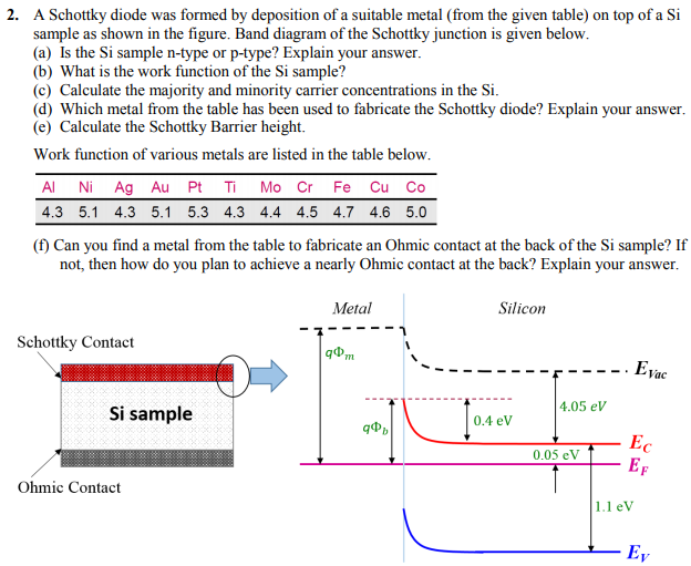
Solved 2. A Schottky diode was formed by deposition of a ...
Schottky Diode - Characteristics, Parameters and Applications Schottky diode is another type of semiconductor diode, but instead of having a P-N junction, Schottky diode has a metal-semiconductor junction and which reduces capacitance This schematic symbol can easily be used to distinguish Schottky diode from other diodes when reading a circuit diagram.

Schottky diode - Definition, Symbol, Working and Applications ...
Schottky Diode Working and Its Applications Schottky diode is also known as barrier diode. Learn more about Schottky diode working, construction, V-I characteristics, features and Due to thermal agitation, some carriers have equal energy to or larger than the conduction band energy to the metal-semiconductor interface, and to the...

Schottky barrier - Wikipedia
Schottky Diode or Schottky Barrier Semiconductor Diode Schottky diodes have many useful applications from rectification, signal conditioning and switching, through to TTL and CMOS logic gates due mainly to their low power and fast switching speeds. TTL Schottky logic gates are identified by the letters LS appearing somewhere in their logic gate circuit...

Figure 1 from A Micro Nuclear Battery Based on SiC Schottky ...
Metal-Semiconductors Contacts - Engineering LibreTexts Figure 1 shows the energy band diagram after the contact is made. Not all MS contact can perform as the rectifying Schottky diode, since there is no potential barrier formed. Under this situation, when the current can be conducted in both directions of the MS contact, the contact is defined as the Ohmic...

Reserach Express@NCKU - Articles Digest
Schottky Diode - Function, Construction, Characteristics, Applications... A Schottky diode, widely popular as barrier diode, refers to a metal-semiconductor diode that comprises lower voltage drops than usual PN-junction diodes. The following diagram represents the Schottky diode symbol -. [Image will be Uploaded Soon]. In the above diagram, the anode section...
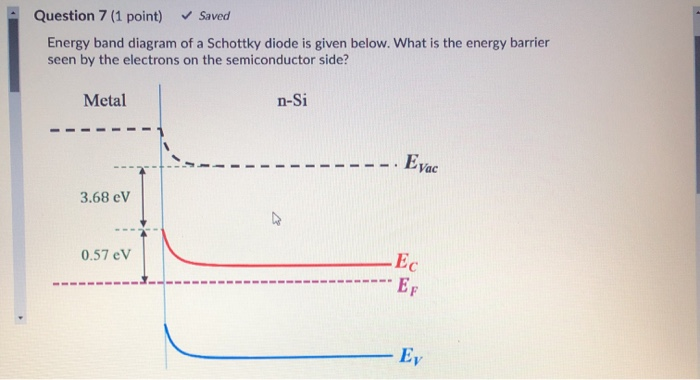
Solved Question 7 (1 point) Saved Energy band diagram of a ...
Schottky Diodes - Working, Characteristics, Application - Homemade... Schottky diodes are constructed differently compared to the traditional p-n junction diodes. Instead of a p-n junction they are built using a metal In Schottky diodes electrons become the majority carrier in the semiconductor material, while in the metal exhibits extremely small minority carriers (holes).

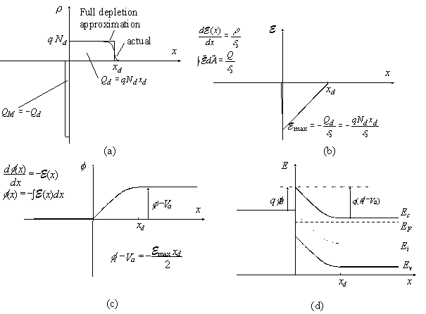
Lecture 7 OUTLINE Poisson's equation Work function Metal ...
PDF Broadband schottky diode 2 Schottky Diode Technology for Frequency Multipliers. 145 5.9 Block diagram for the W -band fundamental mixer measurement. . . . 145 5.10 Measured output power across W -band for 100 mW input power. . . .

Figure 2 from On the Influence of Surface Treatment on ...
GaN-Based Schottky Diode | IntechOpen

THE METAL–SEMICONDUCTOR OR SCHOTTKY JUNCTION - Electronic ...
Micromachines | Free Full-Text | Electrical Characterizations ...
Schottky Diode

Modeling Electrical Properties of Organic Schottky Diodes ...
3.1.6.2 Schottky Contact
Figure 5 from Layer dependence and gas molecule absorption ...
1 Graphene Schottky diodes: an experimental review of the ...
Phanomene elektrischer Kontakte

Schottky Barrier Diode - Power Microelectronics. Device and ...
Semiconductor Junctions, Solid-Solid Junctions | SpringerLink

Band diagram of the Schottky Junction explaining the sensing ...
Lecture contents

Figure 34. I-V characteristics of the Pt/GaOx/GaN-based ...
3.1.6.2 Schottky Contact
Description of transport properties of Schottky diodes ...
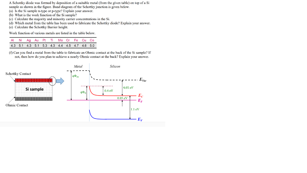
Solved A Schottky diode was formed by deposition of a | Chegg.com
semiconductor physics - Current-voltage characteristics of ...

EE327 Lec 22c Schottky

SSPD_Chapter 3_Section 3.4.Schottky Diode and Section 3.5 ...
Schottky diode
Electronic Physics
0 Response to "36 schottky diode band diagram"
Post a Comment